The core technologies for ASC International's Solder Paste Inspection systems are laser-based or structured white light Moire´ interferometry. Explore the information below to help find the right technology to meet your overall SPI requirements.
Imaging Technologies - SPI
Laser-Based Technology
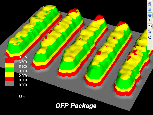
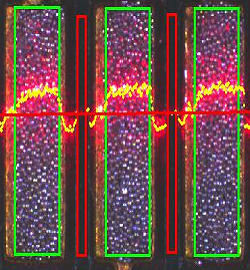
How does laser-based technology work? Utilizing the core principles of laser triangulation, a laser stripe is projected at a specific angle to the imaging camera. As the laser moves across the surface, a string of data is automatically collected from the centroid of the laser stripe generating a differential height reading from the base surface to the overall surface of the solder paste deposit. Single laser stripe SPI systems provide accurate and reliable height characteristics along with 2D cross sectional profiles whereas laser scanning sensor SPI systems can provide accurate and reliable height, area and volume charateristics with more complete 3D profiles for advanced qualitative analysis.


Structured White Light Moiré Interferometry
How does structured white light Moiré interferometry technology work? A known light pattern is projected onto a surface with the image being transferred to a high resolution camera. On a flat surface, the projected pattern image appears to be undistorted to the camera. On a contoured surface such as a freshly printed circuit board, the pattern will follow the height variations from the surface to the solder deposits and this images will appear distorted to the camera. The distorted image is compared with the undistorted image and the difference is directly related to the height of the contoured object at every pixel. Pixel by pixel data replication as provided by this technology offers the most accurate and reliable method for obtaining true 3D, volumetric measurements critical to your overall screen print process strategy.